Single-Transistor Bidirectional Level Shifter
If you have always thought that you need an IC to do bidirectional level shifting, here is a circuit that can do it all using just one FET.
Level shifting is often required to make different electronic boards communicate with each other. Even on the same board it is common to find chips working at different voltages. One good example is I2C: you can find I2C parts working with supplies ranging from as low as 1.5V all the way up to 5V. The I2C protocol is half-duplex, so bidirectional level translation is required.
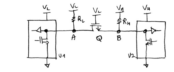
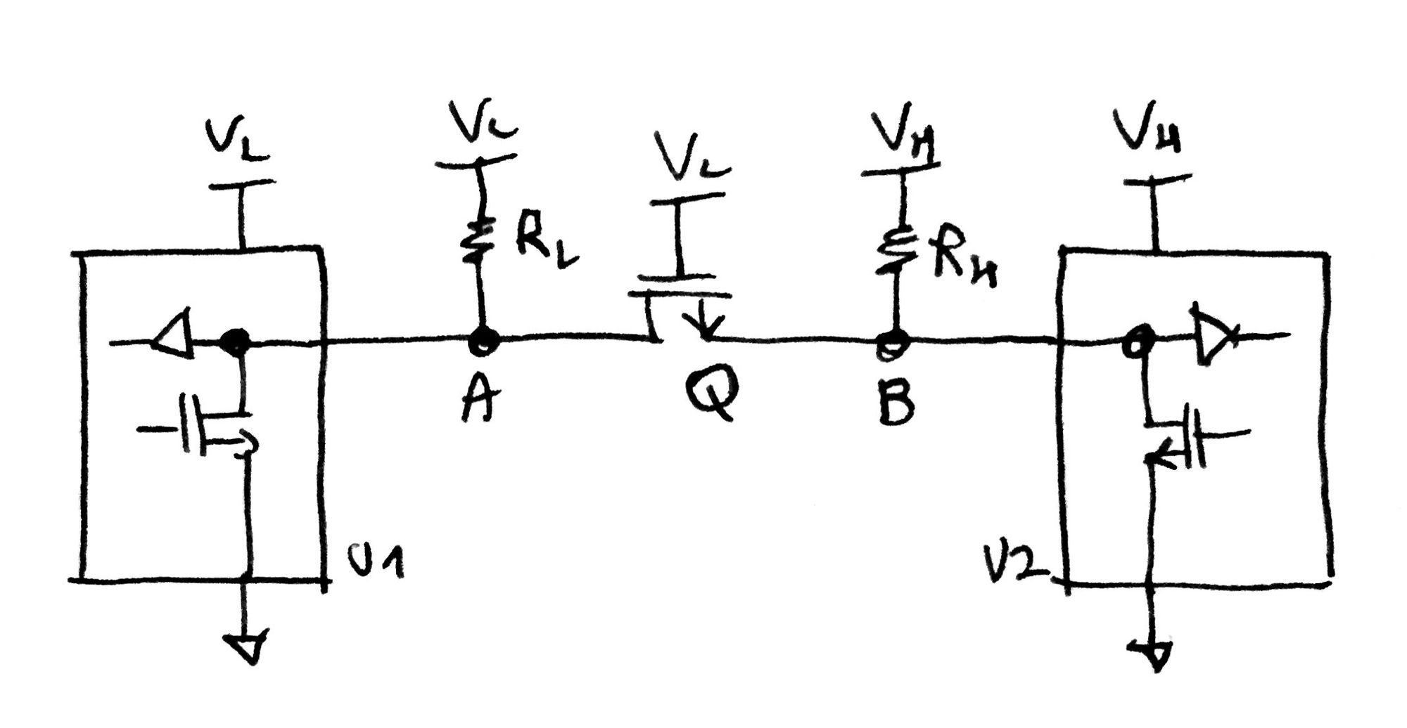
Figure 1 shows a very simple circuit to achieve bidirectional level shifting using a single FET and two resistors. Quite elegant, isn’t it? The two ICs $U_1$ and $U_2$ want to communicate via I2C but they run at different voltages $V_L$ and $V_H$, where $V_L < V_H$. The N-MOSFET Q has the gate biased with $V_L$. Pull-up resistors are applied at each side of the FET, each to their relative supply voltage.
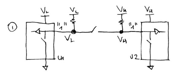
Here is how the circuit works. When $U_1$ wants to transmit a logic "one" it turns off its internal FET thus letting $R_L$ pull the voltage of node A to $V_L$. This will turn-off the FET Q, opening the circuit and allowing B to be pulled to a high voltage, $V_H$ in this case. $U_1$ effectively “transmitted” a logic "one" to $U_2$.
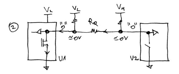
When $U_1$ wants to transmit a logic zero, it pulls A to ground. This turns Q on and begins the discharge of the node B. Eventually both nodes A and B are at the ground potential. A logic zero has been passed from $U_1$ to $U_2$. Note that the same behavior is observed if the direction of the communication is inverted.
I have used this circuit in several projects. It is simple and reliable. However there are few things that needs to be considered before using it:
- If you are using this circuit to translate the voltage level out of a full CMOS output, keep in mind that the voltage will now have a much slower rising edge compared with the falling one. This is due to the fact that the voltage is pulled high not by a strong/low-resistance FET, but instead by a rather large resistance.
- Moreover, the circuit draws constant current when a logic zero is transmitted. Make sure this is compatible with the power budget of your project.
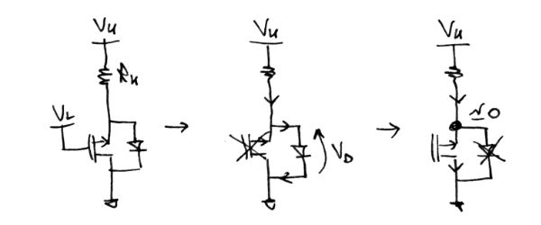
- Commercial FETs are not symmetric. There are several differences between the source and the drain. The biggest difference, as far as this circuit is concerned, is the presence of the body diode. Off-the-shelf transistors usually have the body shorted with the source, and this is represented by a diode in antiparallel with the drain and the source. Figure 4 shows the equivalent circuit when $U_1$ transmits a zero. When $U_1$ pulls A low, the diode turns on first and the voltage across the FET is $V_D$. The FET goes from saturation to ohmic region and causes the diode to turn off. However, if $R_H$ is too small or the FET is too weak, it is possible that the diode never turns off and the FET stays in saturation. This could cause thermal problems for the FET and, more importantly, could make $U_2$ misinterpret the voltage at B ($V_D$) for a logic high. Make sure you size both the resistors and the FET to guarantee that the body diode always turns off.
In conclusion this a useful and elegant way to do level shifting of digital signals between circuits or ICs working in different voltage domains.